JBH crews are completing work under the SSiFR Tool Install at Sandia National Laboratories in Albuquerque, NM supporting the work detailed in the below news release republished in its entirety with approval.
Sandia Labs News Releases
March 25, 2015
MESA complex starts largest production series in its history
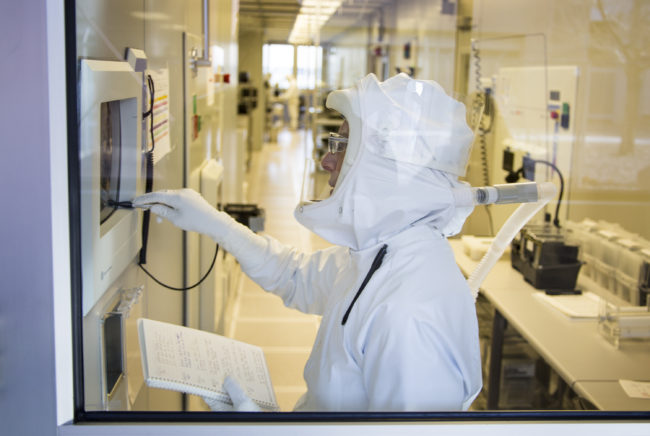
ALBUQUERQUE, N.M. — Sandia National Laboratories has begun making silicon wafers for three nuclear weapon modernization programs, the largest production series in the history of its Microsystems and Engineering Sciences Applications complex.
MESA’s silicon fab in October began producing base wafers for Application-Specific Integrated Circuits for the B61-12 Life Extension Program, W88 Alteration 370 and W87 Mk21 Fuze Replacement nuclear weapons. Planning and preparation took years and involved more than 100 people.
“We left no one untouched. If you were standing still, you got something to do,” said Jayne Bendure, who was in charge of organizing 1,000 line items to be checked off before wafer production began.
Dave Sandison, a senior manager at MESA’s Silicon Fab when the manufacturing readiness process began in July 2011, said detailed requirements for making war reserve-quality Application-Specific Integrated Circuits (ASICs) produced a gigantic list “in regular 12-point font about 4 feet long that went down the wall in my office.”
“It was a multiyear program executed with precision and dedication. I’m very, very proud of the team,” said Gil Herrera, director of Microsystems Science & Technology. “Now the hard part begins: We’ve got to make the parts.”
MESA is center of Sandia’s microsystems work
MESA is the center of Sandia’s investment in microsystems research, development and prototyping. The 400,000-square foot complex of cleanrooms, labs and offices is home to design, development, manufacture, integration and qualification of trusted microsystems for national security applications. MESA includes the Silicon Fab, completed in 1988, and the Compound Semiconductor MicroFab, completed in 2006. The Silicon Fab, certified by the Department of Defense as a trusted foundry, develops and produces technologies for radiation-hardened complementary metal-oxide-semiconductor integrated circuits and micro-electro-mechanical systems. The MicroFab is a green-certified plant for III-V compound semiconductor material processing, post-silicon wafer processing and advanced packaging and for heterojunction bipolar transistor production. Both fabs conduct research and development for future nuclear weapon and national security applications.
Kaila Raby, manager for the ASICs Product Realization Team, said starting production was a huge milestone. The Silicon Fab will make ASICs through 2018 on the plant’s normal schedule of 24 hours a day, five days a week. In addition, the MicroFab is preparing to make heterojunction bipolar transistor integrated circuits in April, the first time MESA will produce those products for the stockpile, Raby said.
Ten different ASIC products go into the three weapon systems, Raby said. Seven of the 10 ASICs have base wafers that are customized into product-specific designs during later production, she said. It’s these base wafers the Silicon Fab started manufacturing.
Sandia has invested in new manufacturing tools and processes for MESA, including 2-D marking, similar to bar-coding, for individual devices; an electronic production control system; automated lot acceptance support systems; streamlined quality management; and a greater focus on preventing defects, Herrera said.
“A lot of things we’ve been working on for the last few years came together, and we’re doing all this while minimizing impacts to our other work for national security customers and the research mission,” he said.
Identifying production needs was multiyear project
MESA Silicon Fab finished wafer fabrication for the W76-1 nuclear weapon in 2009, and began identifying manufacturing needs for the B61 and W88 programs, said fab manager Dale Hetherington.
“A large part of our mission is research and development and work for other customers besides the nuclear weapons program, so while we’ve been getting ready for this [nuclear weapon] production and doing this 1,000 line-item production plan, we’ve still been manufacturing prototypes for the [nuclear weapons] complex, for other missions around Sandia and other labs as well,” Hetherington said. “So it’s not as if we shut down and did nothing but get ready for production.”
Volume for ASIC production will be more than three times that of W76-1 production. MESA uses a build-ahead process: build many wafers and store them so they’re ready when needed.
“We typically build early because the wafers have to be diced into chips, the chips packaged and delivered to subsystem customers, and those subsystems then integrated into higher-level systems,” Hetherington said, adding Sandia has a production plan that factors in all the various chips for the B61, W88 and W87 Mk21 fuze programs.
Wafer production is a critical part of the ASIC process but is only one step toward the final product and acceptance by the National Nuclear Security Administration. “While we build the wafers in our fab, when we’re done with them they have to be electrically tested, they need burn-in and reliability evaluation, they need packaging, so there’s multiple sets of work activities from initial customer engagement through the design phases and into manufacturing,” said fab manager Alan Mitchell.
Senior manager Paul Raglin said MESA’s fabs are unique: They do research and development and production of ASICs and heterojunction bipolar transistors, all in-house with trusted components. “We can go directly into the stockpile with all the certifications,” he said.
MESA receives about $50 million a year through the National Nuclear Security Administration’s Readiness in Technical Base and Facilities, Raglin said. The W88 and B61 programs furnish additional money for staff and materials above this base-level funding.
The Sandia silicon fab revitalization program has pledged $150 million over seven years to replace aging tools and to transition MESA to 8-inch wafers by about 2020, Raglin said.
Sandia National Laboratories is a multi-program laboratory operated by Sandia Corporation, a wholly owned subsidiary of Lockheed Martin Corp., for the U.S. Department of Energy’s National Nuclear Security Administration. With main facilities in Albuquerque, N.M., and Livermore, Calif., Sandia has major R&D responsibilities in national security, energy and environmental technologies and economic competitiveness.